Building a smart fan controller with Raspberry Pi
Designing a Digital-to-Analog Control Circuit for Fan Speed
At this stage, we've designed an optocoupler SSR controller to manage both forward and reverse operation of our VFD from the Raspberry Pi. It also controls a larger mains relay to completely switch the VFD on and off. Now, we need to address the speed control interface. This step is a bit more complex than the simple switching circuits using the SSR!
As mentioned previously, we decided to interface with the VFD's speed control using a 0-10v control signal, as this is the industry standard for lower-end systems. But how do we generate this analog signal from the digital Raspberry Pi? The solution is to use a Digital-to-Analog Converter, or DAC. A DAC allows us to take the digital signal from the Raspberry Pi and convert it into an analog voltage, which is perfect for controlling the VFD's speed.
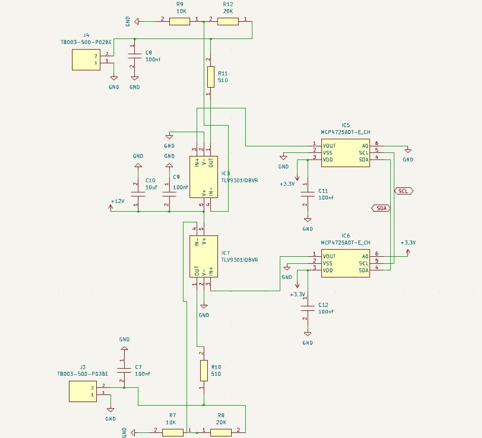
I've designed the following schematic to generate our 0-10V signal. It includes a DAC that feeds an operational amplifier (op-amp) with a gain of 3. This amplifies the DAC's maximum 3.3V output (its positive rail voltage) to around 9.9V—essentially, 10V for the VFD.

The DAC Stage
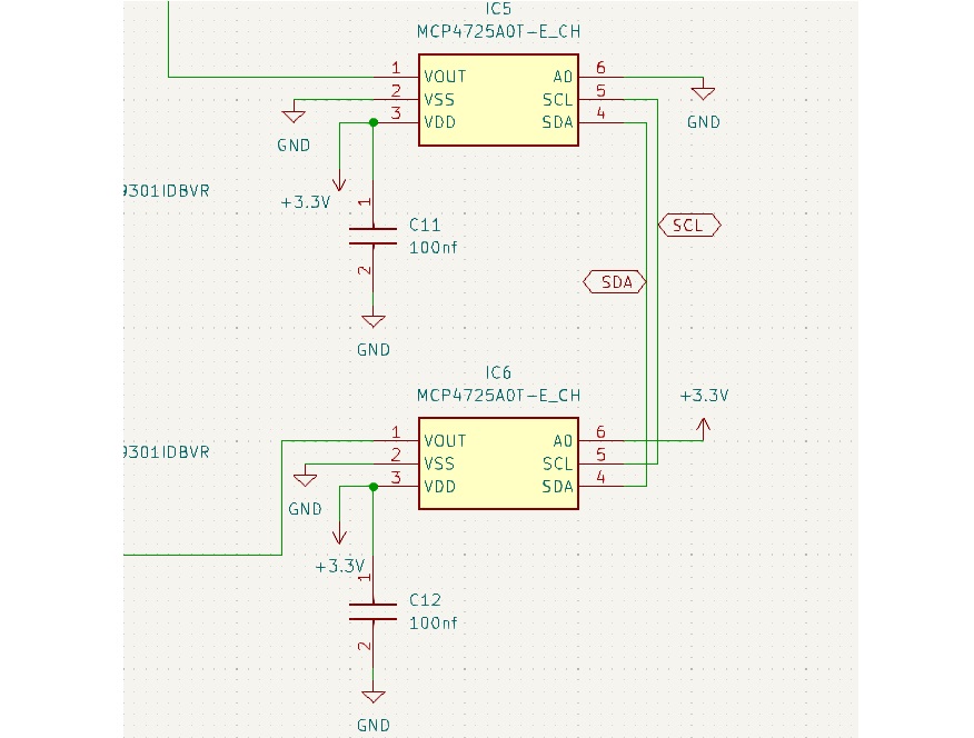
Let's start by looking at just the DAC stage of the 0-10V generation. This is where we take in an I2C digital signal (via the SCL and SDA lines) from the Raspberry Pi and convert it into a analog signal.

For the DAC, I've chosen the MCP4725A0T. It offers 12-bit resolution, giving us 4096 discrete levels within the 0-3V range. This means each step is around 0.00073V, giving us precise control over the output. The DAC can be powered from 2.7V to 5.5V, so it works seamlessly with our 3.3V supply, which powers other components on our board—no need for a separate power supply.
Its rail-to-rail operation allows us to get very close to 3.3V on the output, maximizing the voltage range.
I duplicated the DAC circuit because I might want to control two VFDs. This is easy: by tying one A0 pin (address 0) to GND and the other to 3.3V, we give each DAC a unique I2C address. The base address of the DAC is 1100000, where the LSB is A0. By setting one high and one low, we get two addresses: 1100000 (0x60) and 1100001 (0x61).
Now we have two DACs, each outputting an analog voltage of 0-3.3V. But we need 0-10V, not 0-3.3V, right? That's where the second stage of our circuit comes in: we need something to boost the 0-3.3V range to 0-10V.
Using an Operational Amplifier
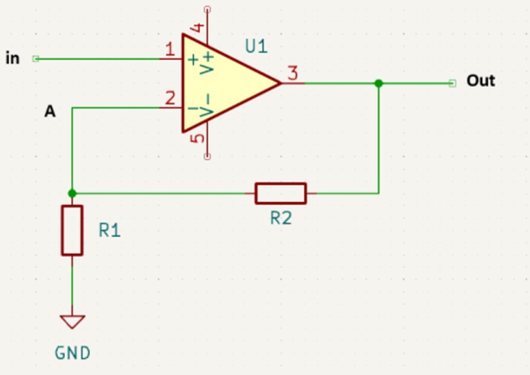
For this, we use an operational amplifier (op-amp), specifically a non-inverting amplifier with a gain of around 3.
Here's the basic diagram for a non-inverting amplifier:

The gain is determined by the equation
Final Circuit Design
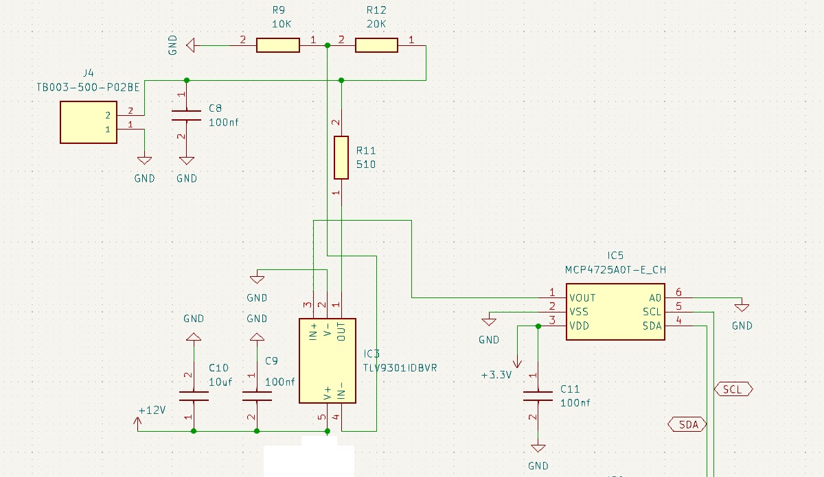
The circuit diagram below shows just one side of the complete DAC-to-op-amp-to-output circuit for simplicity; the other side mirrors it. I've selected the TLV9301 op-amp because it offers rail-to-rail operation and can supply up to 60mA of output current.

The op-amp is powered by a 12V supply, with the 3.3V DAC output as the input. The resistors R9 and R12 form the voltage divider, giving a gain of 3. We've also added a small stabilizing capacitor (C8) on the output to smooth any potential transients—though this may not be strictly necessary, it feels like a good precaution.
Most op-amps don't like a direct capacitor connection on their output, but they tolerate it better if a resistor is placed in series. This is where R11 comes in. It limits the output current to about 20mA (at the 10V maximum) to prevent damaging the op-amp. It also ensures stability by avoiding direct connection between the capacitor and op-amp output.
Side note: There's a minor issue in the schematic with R11. With a resistance of 510Ω, it forms a voltage divider with the output, which results in slightly higher gain than we want. This can be fixed by moving R11 out of the feedback loop of the op-amp. However, I didn't catch this until after ordering the PCB, so I've left it in the schematic for now.